


This article was automatically translated from the original Turkish version.
+2 More
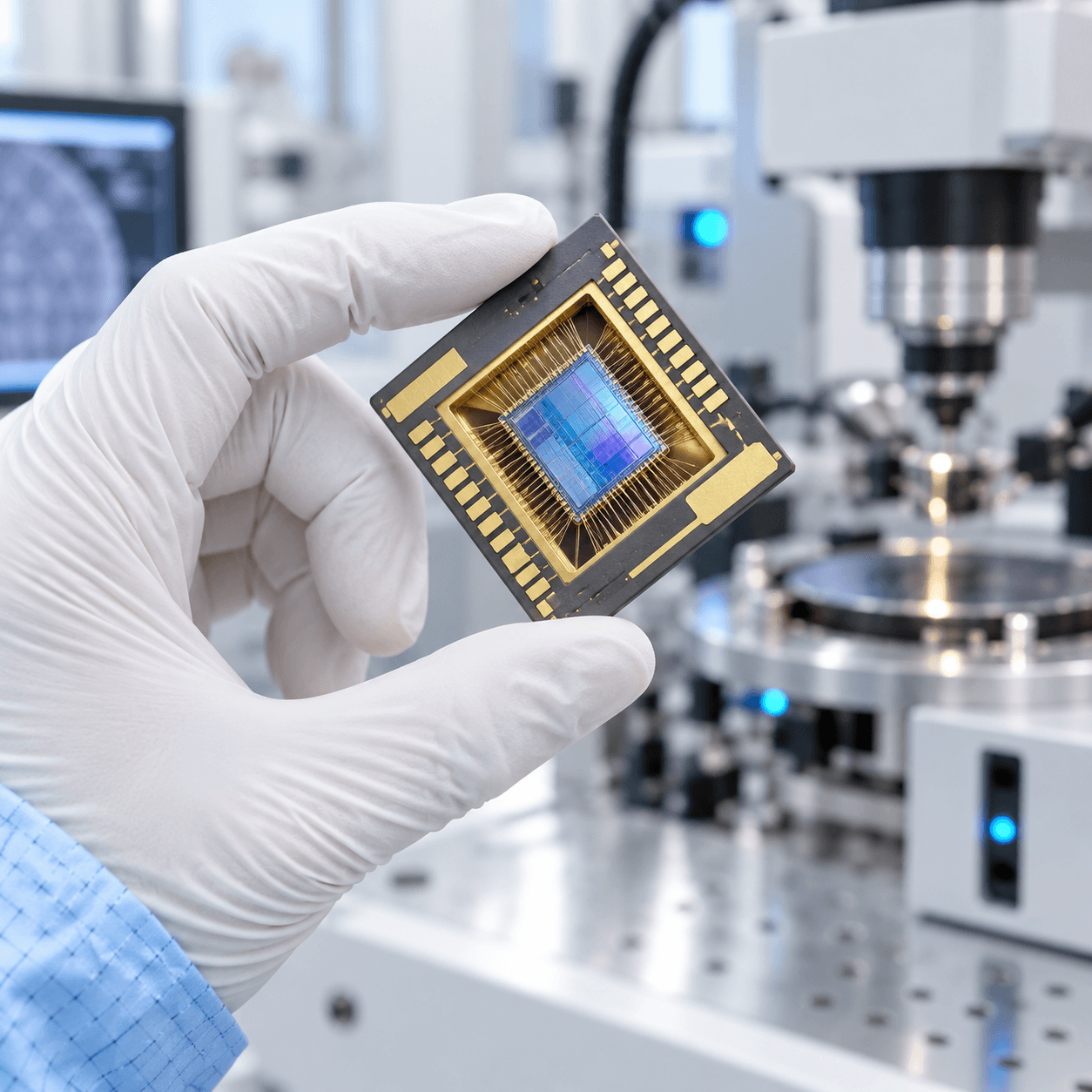
Semiconductor Technologies Research Laboratory (Generated with Artificial Intelligence.)
Full Name | Semiconductor Technologies Research Laboratory | ||||||||
|---|---|---|---|---|---|---|---|---|---|
Abbreviation | YİTAL | ||||||||
Foundation Date | 1983 | ||||||||
Place of Foundation | Gebze, Kocaeli | ||||||||
Affiliated Institution | TÜBİTAK BİLGEM | ||||||||
Affiliated Institute | National Electronics and Cryptology Research Institute (UEKAE) | ||||||||
Areas of Activity | Semiconductor technologies and integrated circuit design/manufacturing | ||||||||
Production Technologies | 0.25 µm 5-metal CMOS; 0.25 µm 5-metal SiGe BiCMOS | ||||||||
Production Scope | Design, photomask, pulping, testing, packaging and aging | ||||||||
Notable Works | Cryptographic integrated circuits, smart card, 8051 processor, photodetectors, RF and NTDS | ||||||||
Semiconductor Technologies Research Laboratory (YİTAL) is a research laboratory under the National Electronics and Cryptology Research Institute (UEKAE), which operates within TÜBİTAK BİLGEM. The laboratory conducts research on the development of semiconductor manufacturing processes as well as integrated circuit (IC) design and production. Established in 1983, YİTAL possesses an integrated production infrastructure encompassing IC design, photomask fabrication, silicon wafer processing, on-wafer testing, packaging, circuit testing, and aging stages.【1】
The laboratory was established to build expertise in microelectronics, carry out research and development activities for industry, and develop integrated circuits of strategic importance. Since its founding, it has developed CMOS and SiGe-based manufacturing processes and worked on cryptographic ICs, photodetectors, processors, and RF circuits. The laboratory’s current activities focus on developing original production technologies to meet Türkiye’s strategic semiconductor needs and producing ICs using these technologies.【2】
Institutional initiatives targeting semiconductor production in Türkiye became prominent in the late 1970s. During this period, the Turkish Electronics Industry and Trade Inc. (TESTAŞ), established to develop the domestic electronics industry, planned to create a Semiconductor Circuit Element Factory (YİDEF). A 7 µm bipolar manufacturing technology was transferred from the United States, and personnel received training abroad to utilize this technology. To support YİDEF’s production activities, resolve technical issues arising during manufacturing, and conduct research on new semiconductor technologies, the establishment of a dedicated research infrastructure under TÜBİTAK was proposed.【3】
In this context, YİTAL was established in 1983 within the Marmara Research Center of TÜBİTAK in Gebze. The laboratory’s initial efforts focused on adapting the bipolar manufacturing technology acquired from TESTAŞ to local conditions; various analog ICs included in the technology package were produced at YİTAL.【4】
From the late 1980s, YİTAL’s research shifted toward CMOS (Complementary Metal-Oxide-Semiconductor) technology. Under the NATO-TU-MICROFAB project, supported by NATO’s Science for Stability program and involving TÜBİTAK, Istanbul Technical University, and TELETAŞ, the necessary technological knowledge and infrastructure for CMOS IC production were developed. During the project, YİTAL expanded its silicon wafer processing capacity and added new production and measurement equipment required for CMOS manufacturing to its infrastructure.【5】
As a result of the NATO-TU-MICROFAB project, YİTAL developed a 3 µm CMOS manufacturing process. This process encompassed not only transistor fabrication but also complementary stages such as design rule development, circuit modeling, photomask fabrication, and prototyping of integrated circuits. Using this developed technology, application-specific ICs were produced for the domestic electronics industry. Subsequent efforts reduced the production geometry, achieving a 1.5 µm CMOS technology by 1998.【6】
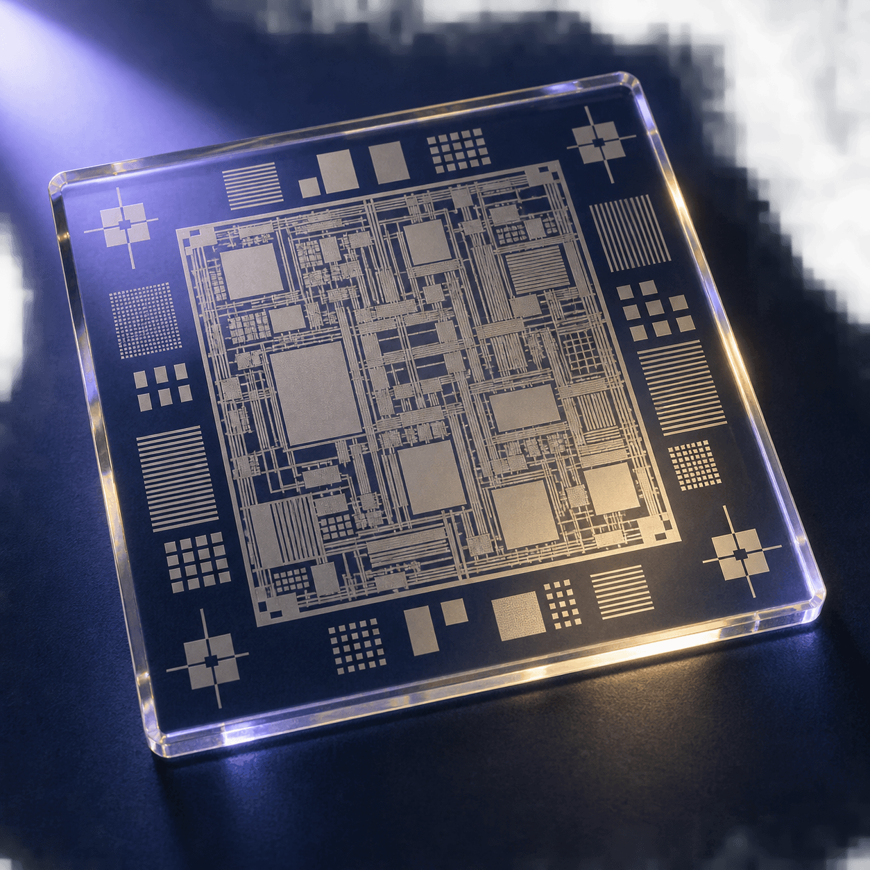
Tümdevre Desenlerini Silisyum Pula Aktarmada Kullanılan Fotomaske (Yapay Zeka ile Oluşturulmuştur.)
YİTAL’s production infrastructure was upgraded in 2000 to support higher-capacity IC production. Between 2002 and 2005, a 0.7 µm CMOS manufacturing process was developed and applied to produce application-specific ICs (ASICs) for UEKAE’s cryptographic systems. In 2007, IC production at the 0.35 µm level was achieved with a 20 V CMOS process; in 2008, a 24 V CMOS process was developed for high-voltage applications.【7】
According to TÜBİTAK BİLGEM’s institutional chronology, in 2021 YİTAL developed 0.25 µm (250 nm) 5-metal CMOS and 0.25 µm 5-metal SiGe BiCMOS chip manufacturing technologies.【8】
In 2007, YİTAL initiated research to develop SiGe HBT and BiCMOS technologies alongside its existing 0.35 µm CMOS process. Silicon-germanium (SiGe)-based heterojunction bipolar transistors (HBTs) are notable for their performance in high-frequency applications, while BiCMOS technology enables the integration of bipolar transistors and CMOS circuits within the same manufacturing process.【9】
These efforts continued in 2014 with the 0.25 µm (250 nm) SiGe:C BiCMOS Cell Library Development Project, supported by the then Directorate of R&D of the Undersecretariat for Defense Industries. Within this project, in 2018 a npn SiGe HBT process with a cut-off frequency exceeding 120 GHz was developed and its repeatability demonstrated. In 2019, a 0.25 µm CMOS process compatible with this HBT process was developed. By combining the CMOS and SiGe:C processes, YİTAL established its SiGe BiCMOS manufacturing technology and transitioned to producing RF ICs for X-band applications.【10】
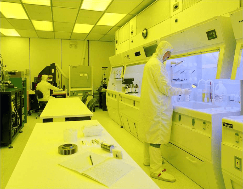
Yarı İletken Üretiminde Kullanılan Temiz Alanlar (Picryl)
Due to the extremely small scale of circuit structures in semiconductor manufacturing, contamination from dust and other particles must be strictly controlled. Therefore, a significant portion of production is carried out in clean rooms where airborne particle concentrations are regulated. YİTAL has a clean room infrastructure of approximately 1,000 m², comprising Class 10 and Class 100 areas. According to TÜBİTAK BİLGEM’s current definition, this infrastructure enables all stages of IC development—including IC design, mask fabrication, IC production, wafer probing, packaging, circuit testing, and aging—to be conducted within the same facility.【11】
YİTAL’s production infrastructure employs semiconductor manufacturing processes such as lithography, ion implantation, thin film deposition, etching, high-temperature treatments, and surface planarization to process silicon wafers. These processes are performed sequentially to fabricate transistors, interconnects, and other structures on the silicon substrate. The 2021 special issue of BİLGEM Technology states that YİTAL’s 0.25 µm SiGe BiCMOS process consists of 33 masks and approximately 300 process steps, and that the laboratory had an annual silicon wafer processing capacity of about 2,500 wafers during the same period.【12】
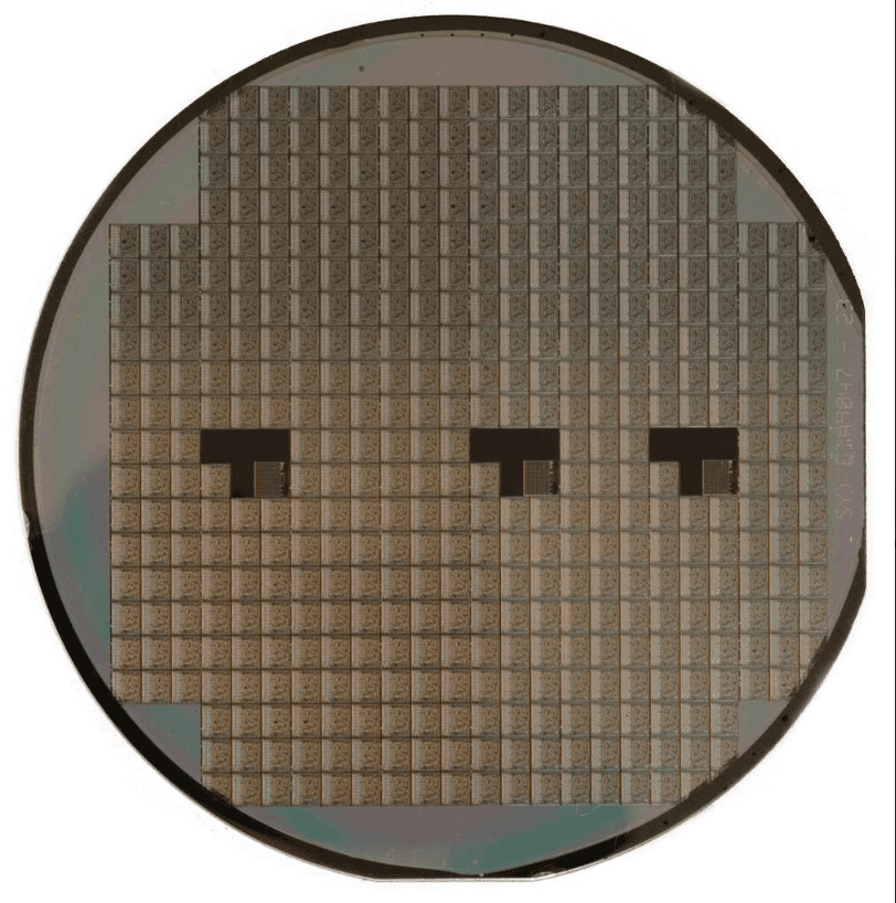
Üzerinde Çok Sayıda Tümdevre Bulunan İşlenmiş Bir Silisyum Pul (Wafer) Örneği (Picryl)
ICs to be produced at YİTAL are designed within the technical limits and design rules of the laboratory’s available manufacturing technologies. The laboratory supports the design of digital, analog, and radio frequency (RF) circuits and develops design tools and cell libraries specific to its manufacturing processes.【13】
After design completion, patterns corresponding to the circuit layers are prepared for production, and photomasks are fabricated to transfer these patterns onto silicon wafers. YİTAL’s mask fabrication infrastructure enables the physical realization of designed ICs within the laboratory.【14】
The physical structure of the IC is formed by layering the designed patterns onto the silicon wafer. At YİTAL, this involves processes such as photolithography, doping, film deposition, etching, and surface planarization. During photolithography, patterns on the photomask are transferred onto a photo-sensitive layer on the wafer surface; subsequent steps then create the necessary regions for transistors and interconnects.【15】 These steps are repeated multiple times using different masks and process sequences according to the IC’s structure. YİTAL’s clean room and production infrastructure enable these stages to be carried out sequentially within the same facility.【16】
Once production is complete, ICs on the silicon wafer undergo wafer probing to test their electrical properties. Circuits meeting production criteria are then separated from the wafer, packaged, and retested. YİTAL’s infrastructure also includes burn-in testing capabilities.【17】
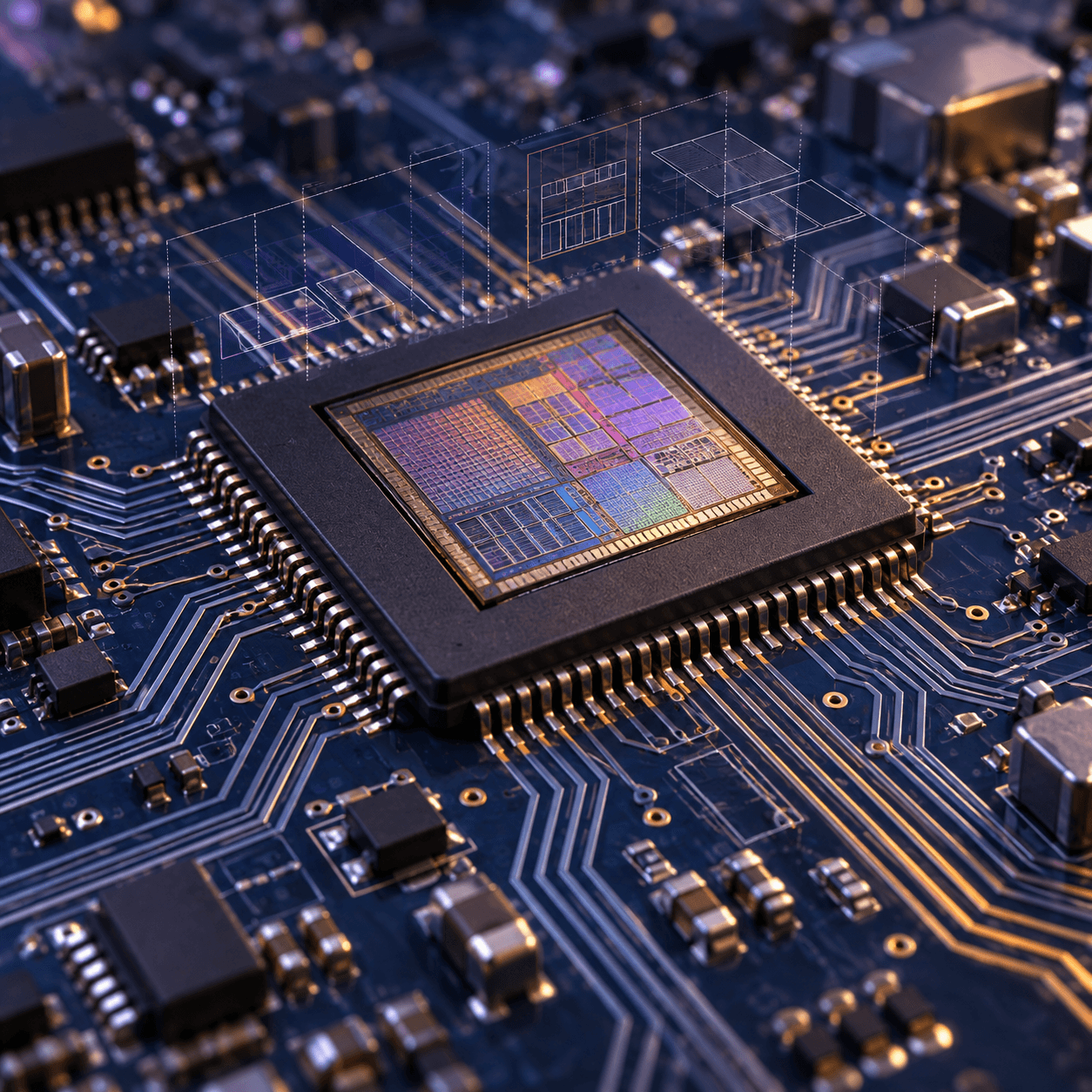
YİTAL’ın 0,25 µm SiGe BiCMOS Proses Tasarım Kitini Simgeleyen Temsili Görsel (Yapay Zeka ile Oluşturulmuştur.)
According to TÜBİTAK BİLGEM’s current data, YİTAL’s production infrastructure includes 0.25 µm (250 nm) 5-metal CMOS and 0.25 µm 5-metal SiGe technologies. The 0.25 µm value corresponds to 250 nanometers and represents the technology node of the semiconductor manufacturing process used.【18】
YİTAL’s 0.25 µm CMOS infrastructure is used for digital IC production, while its 0.25 µm SiGe BiCMOS infrastructure is primarily applied to develop ICs for RF and X-band applications.【19】
In the semiconductor industry, mature nodes with larger geometries address different needs than the smaller nodes used in the most advanced processors. For example, under the United States’ CHIPS program, two new fabrication facilities supported for Texas Instruments are expected to produce analog and embedded semiconductor devices in the 65–130 nm range, along with products such as power management ICs, microcontrollers, amplifiers, and sensors using these processes.【20】 Similarly, investments to modernize and expand Analog Devices’ fabrication facilities in the United States include relocating 180 nm and 350 nm manufacturing processes to the U.S. to produce semiconductor devices for automotive, industrial, and defense applications.【21】
RF applications also exemplify the current use of mature nodes. GlobalFoundries announced in 2025 that it will launch a production version of its 130 nm SiGe BiCMOS platform for communication infrastructure, optical networks, satellite communications, industrial applications, and high-frequency radar systems. YİTAL’s use of its 250 nm SiGe BiCMOS technology in RF and radar circuits demonstrates that the size of a technology node alone does not determine its functionality.【22】
Advanced digital circuits such as processors, graphics processors, and AI accelerators requiring high transistor densities have reached much smaller manufacturing nodes. TSMC’s 3 nm technology entered high-volume production in 2022, and its 2 nm (N2) technology is scheduled to begin high-volume production in the final quarter of 2025. From this perspective, YİTAL’s 250 nm manufacturing technology is significantly behind the current technology nodes used for advanced digital logic circuits.【23】 However, comparing 250 nm nodes with 2 or 3 nm nodes solely based on numerical differences is misleading. Today, the node names used by manufacturers do not directly correspond to a single physical dimension on the transistor.【24】
Therefore, YİTAL’s current technological position must be evaluated from two perspectives. While 250 nm is well behind the cutting-edge nodes used for high-density digital processors, mature manufacturing processes continue to be used for analog, RF, sensor, microcontroller, and similar specialized applications. YİTAL’s production capability should be assessed not only by node size but also by the nature of the circuits it can produce and their intended applications.【25】
One of YİTAL’s early applications was the development of cryptographic ICs for secure communication systems. Digital ICs implementing cryptographic algorithms developed by UEKAE were designed at YİTAL in 1999 and began production using the laboratory’s proprietary CMOS technology, subsequently being deployed in UEKAE’s cryptographic devices. TÜBİTAK BİLGEM notes that tens of thousands of digital ICs produced at YİTAL are actively used in the field.【26】
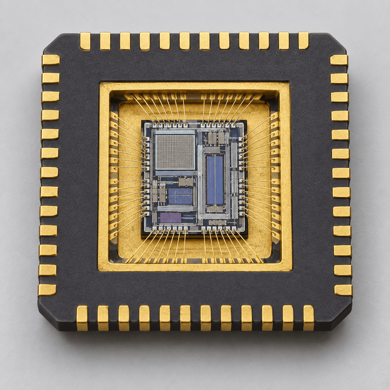
Bir Tümdevrenin Kılıf İçine Yerleştirilmiş ve Altın Tel Bağlantıları Yapılmış Temsili Görünümü (Yapay Zeka ile Oluşturulmuştur.)
YİTAL’s work in secure IC design extended to smart card technologies. As part of the SCARD project under the European Union’s Sixth Framework Programme, YİTAL conducted research on circuit designs resistant to side-channel attacks and launched the National Smart Card IC Design Project in 2006. The first ICs designed were physically manufactured at overseas semiconductor facilities; approximately 20,000 cards were distributed in Bolu during field trials.【27】
In 2011, YİTAL designed and launched Türkiye’s first National Smart Card IC. Subsequent versions of this IC were developed, achieving EAL5+ security certification. Work was also conducted on a dual-interface national smart card design supporting both contact and contactless usage. The physical production of some National Smart Card ICs designed by YİTAL was carried out at overseas semiconductor fabs.【28】
In smart card research, protection of the IC against physical tampering and information leakage was also addressed. YİTAL developed a security method called “Active Shield” for the National Smart Card IC (UKTÜM), which detects physical intrusions by monitoring metal interconnects on the chip surface. This solution was patented by the United States Patent and Trademark Office in 2015.【29】
Another group of semiconductor products developed at YİTAL is photodetectors. The laboratory developed manufacturing processes for photodetectors and began supplying four-region photodetectors from 2010. These detectors use four sensing regions fabricated on a single silicon substrate to determine the position of incoming laser light. YİTAL’s product line includes four-region photodetectors with different characteristics as well as laser proximity sensors.【30】
These products have found particular use in defense applications. In a 2017 statement, TÜBİTAK indicated that semiconductor detectors developed at YİTAL are used in the seekers of munitions such as MAM-L and CİRİT. The special issue of BİLGEM Technology on semiconductor technologies lists MAM-L, MAM-C, CİRİT, and LUMTAS munitions among their application areas.【31】
YİTAL has not only developed detectors that sense light but also the readout circuits that process the electrical signals from these detectors. According to TÜBİTAK BİLGEM’s current information, circuits processing data from photodetectors and laser proximity sensors are produced using YİTAL’s 0.7 µm 2-metal CMOS technology.【32】
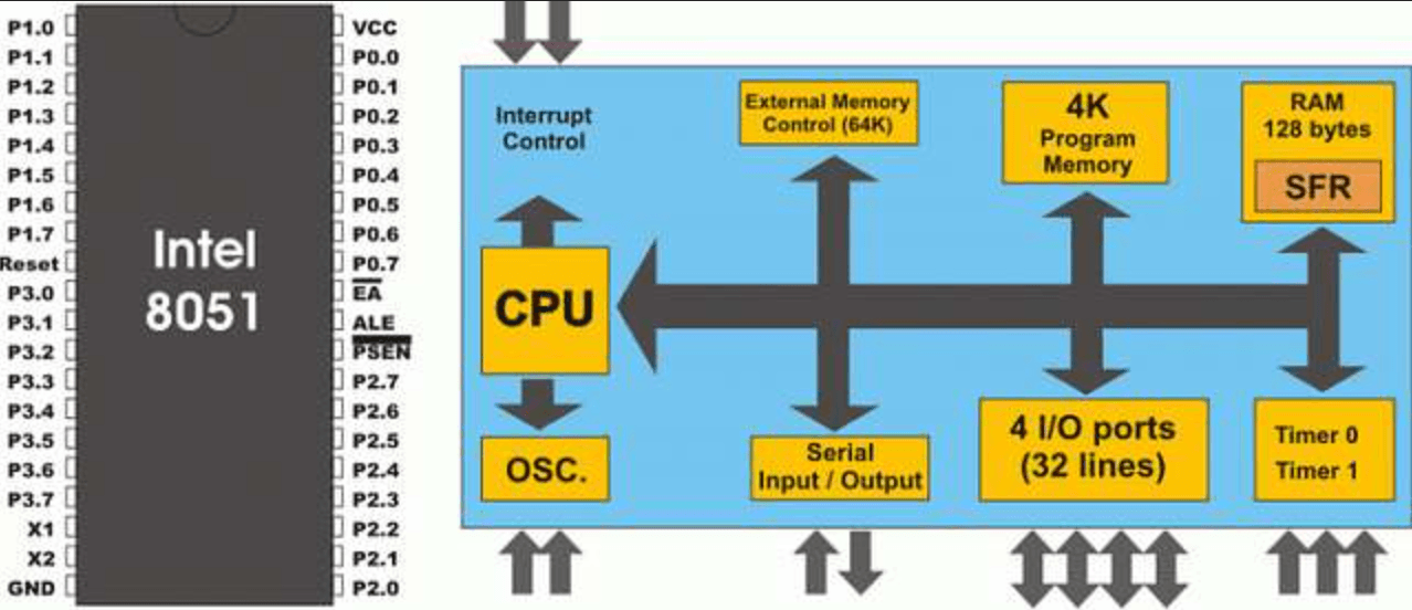
8051 Mimarisine Dayalı Bir Mikrodenetleyicinin İşlevsel Yapısı (Picryl)
One of the products of YİTAL’s digital IC research is a processor based on the 8051 architecture. The processor was designed at YİTAL, manufactured using the laboratory’s 0.25 µm (250 nm) 5-metal CMOS technology, and packaged. TÜBİTAK BİLGEM identifies this processor as Türkiye’s first domestically produced processor. Its maximum operating frequency is 17 MHz, with a power consumption of 25 mW.【33】
TÜBİTAK BİLGEM also states that research is underway to develop custom multi-core processors for specialized applications, including the creation of processor-specific machine language, compilers, simulators, and development environments.【34】
One of the primary application areas of YİTAL’s SiGe BiCMOS manufacturing technology is radio frequency (RF) integrated circuits. The development of the 0.25 µm SiGe BiCMOS technology aimed to enable domestic production of RF circuits in X-band radar transceivers used in Türkiye. This technology allows the integration of digital and analog CMOS circuits with high-frequency SiGe circuits on the same chip.【35】
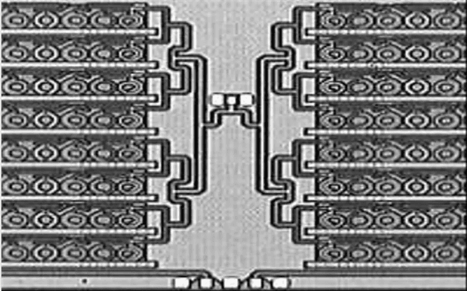
SiGe BiCMOS Teknolojisiyle Geliştirilmiş Bir Radyo Frekans Güç Yükselteci (Picryl)
One application-oriented project using this technology is the design of a low-noise amplifier (LNA) for the X-band. The HBT modeling and X-band differential low-noise amplifier work conducted by YİTAL researchers using the 0.25 µm SiGe:C BiCMOS process received the Best Paper Award at the 22nd International Mediterranean Microwave Symposium in 2023.【36】
Another application of YİTAL’s high-voltage CMOS work is the development of the NTDS (Naval Tactical Data System) interface communication IC and card. The ICs used in NTDS cards were manufactured using the 24 V high-voltage CMOS process developed at YİTAL. Thus, a specialized CMOS manufacturing technology developed in the laboratory was adapted for a naval tactical data communication application.【37】
Today, YİTAL operates as a research laboratory under the National Electronics and Cryptology Research Institute (UEKAE), which is part of the TÜBİTAK Center for Information and Information Security Advanced Technologies (BİLGEM). While UEKAE conducts research and development in electronics, cryptography, and information security, YİTAL focuses within this structure on semiconductor manufacturing technologies and IC development.【38】
To scale up semiconductor technology research and production activities to industrial levels, YİTAL Mikroelektronik Sanayi ve Ticaret A.Ş. was established on September 25, 2017. The company’s capital was distributed as follows: 51% to ASELSAN, 29% to TÜBİTAK, and 20% to the then Undersecretariat for Defense Industries. The company was established with the goal of operating in the micro- and nanoscale device field and becoming a “trusted semiconductor foundry.”【39】
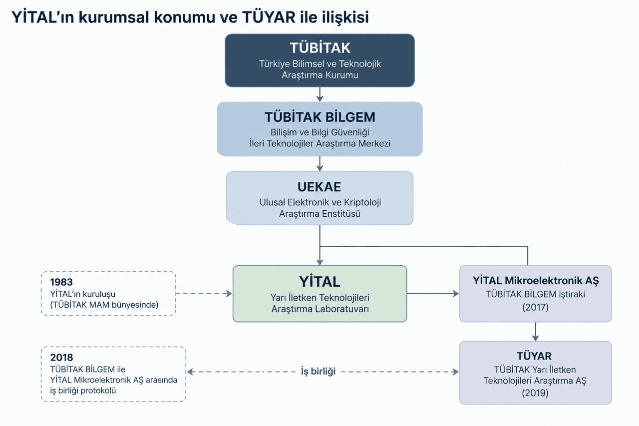
YİTAL’ın Kurumsal Konumu ve TÜYAR ile İlişkisi (Yapay Zeka İle Oluşturulmuştur.)
In 2018, a collaboration agreement was signed between TÜBİTAK BİLGEM and YİTAL Mikroelektronik A.Ş. The agreement aimed to expand semiconductor and microelectronics research, foster the development of a domestic ecosystem in this field, and transfer developed technological capabilities to industry. One of the stated goals was to enable the production, packaging, and testing of critical microprocessors designed in Türkiye without outsourcing these steps abroad.【40】
On May 8, 2019, the company’s name was changed to TÜYAR Mikroelektronik Sanayi ve Ticaret A.Ş. during an ordinary general assembly. The establishment of the company did not signify the end of the YİTAL research laboratory. TÜBİTAK’s official announcement confirmed that the laboratory would continue its scientific activities. YİTAL remains part of UEKAE’s research laboratories today. TÜYAR’s current activities focus on chip packaging solutions, offering services ranging from prototyping to low-volume and high-volume production in the application-specific packaging domain. Thus, the YİTAL laboratory and the company now known as TÜYAR are distinct organizational entities.【41】
Türkiye’s current semiconductor infrastructure comprises diverse structures ranging from research centers to private sector initiatives, covering IC design to production. The 2030 Industry and Technology Strategy identifies YİTAL within TÜBİTAK BİLGEM, alongside ODTÜ MEMS and ASELSAN Bilkent Micro Nano Technologies Industry and Trade Inc., as key entities active in this field.【42】
One distinguishing feature of YİTAL within this structure is that its activities extend beyond IC design to include development of manufacturing processes, physical production, and testing. In this context, the laboratory provides infrastructure for low-volume and application-specific IC production using proprietary CMOS and SiGe manufacturing processes.【43】
In Türkiye’s current policies regarding semiconductor and IC technologies, developing domestic design and production capabilities, reducing dependence on foreign critical components, and strengthening existing research infrastructure are key priorities. The 2030 Industry and Technology Strategy identifies semiconductor technologies as one of the strategic areas for developing high-tech production capacity.【44】
The strategy anticipates the development of an IC design ecosystem, expansion of production capacity, and support for investments targeting critical semiconductors needed by industry. Türkiye aims to support its existing IC design capabilities with serial production infrastructure. By 2028, the goal is to transition to a 110 nm IC manufacturing technology and enable domestic production of critical semiconductors such as identity and passport chips. Additionally, international collaborations aim to establish a 16 nm IC production line and build capacity for producing high-tech chips domestically.【45】
These targets are presented not as a specific roadmap for YİTAL but as national goals for enhancing Türkiye’s overall semiconductor production capacity. The strategy also anticipates strengthening existing competencies within TÜBİTAK.【46】
The HIT-Çip program has allocated a budget of five billion dollars to support semiconductor investments, aiming to bring 65 nm or more advanced technologies to Türkiye through large-scale production facilities. The program also covers investments across different stages of the value chain, including silicon ingots, silicon wafers, testing, and packaging.【47】
2030 Industry and Technology Strategy aims, through the National Chip Consortium, to develop an ecosystem encompassing design, production, packaging, and testing, while strengthening the number of domestic suppliers, qualified human resources, and research infrastructure. YİTAL’s research capacity, focused on low-volume, application-specific ICs and process development, differs in scale and function from the high-volume serial production investments envisioned in policy documents. In this regard, the laboratory constitutes one of Türkiye’s current components in the semiconductor ecosystem, particularly in process development, application-specific IC production, and research infrastructure.【48】
ASELSAN. *30 Eylül 2019 Tarihi İtibarıyla Özet Konsolide Finansal Tablolar*. 2019. Accessed August 30, 2026.https://cdn.aselsan.com/aselsanweb-prod/documents/investor-relations/reports/finansal/tr/report-finansal-09-2019-2019-tr.pdf.
Ataman, Atilla. “Mikroelektronikteki Gelişmeler ve YİTAL’de Geliştirilen 3 µm-CMOS Prosesi.” *Elektrik Mühendisliği 6. Ulusal Kongresi Bildirileri*, 462–470. Bursa, September 11–17, 1995. Accessed August 30, 2026.https://www.emo.org.tr/ekler/6c3b4d7cbc4b727_ek.pdf.
Defense Advanced Research Projects Agency (DARPA). “DARPA Amplifier on Silicon MIT.” March 5, 2013. PICRYL. Accessed September 16, 2026.https://picryl.com/media/darpa-amplifier-on-silicon-mit-b898df.
GlobalFoundries. “GlobalFoundries Announces Production Release of 130CBIC SiGe Platform for High-Performance Smart Mobile, Communication and Industrial Applications.” August 28, 2025. Accessed August 30, 2026.https://gf.com/news-and-events/news/globalfoundries-announces-production-release-of-130cbic-sige-platform-for-high-performance-smart-mobile-communication-and-industrial-applications/.
Inductiveload. “Silicon Wafer.” July 16, 2010. PICRYL. Accessed September 16, 2026.https://picryl.com/media/silicon-wafer-cfbdb6.
Intel. “Accelerating Process Innovation.” July 26, 2021. Accessed August 30, 2026.https://download.intel.com/newsroom/2021/client-computing/accelerating-process-innovation.pdf.
Kaydırma, Hasan, Ahmet Unutulmaz, Nurettin Yaman Özelçi et al. “YİTAL’de Tümdevre Tasarımı.” BİLGEM Teknoloji 11 (January 2021): 72–75. Accessed August 30, 2026.https://en.bilgem.tubitak.gov.tr/wp-content/uploads/sites/8/bilgem_teknoloji_dergisi-11.sayi_.pdf.
Microe. "Microcontroller 8051." March 1, 2015. PICRYL. Accessed August 30, 2026.https://picryl.com/media/microcontroller-8051-5bc10d.
NASA Glenn Research Center. “Silicon Carbide Growth Facility - Clean Room Facility and Surface Analytical Labs.” 1998. PICRYL. Accessed August 30, 2026.https://picryl.com/media/silicon-carbide-growth-facility-clean-room-facility-and-surface-analytical-e235f6
National Institute of Standards and Technology. “Analog Devices Inc. (Washington).” *CHIPS for America*. Accessed August 30, 2026.https://www.nist.gov/chips/analog-devices-inc-washington-camas.
National Institute of Standards and Technology. “Texas Instruments (Texas).” *CHIPS for America*. Accessed August 30, 2026.https://www.nist.gov/chips/texas-instruments-texas-sherman.
T.C. Ministry of Industry and Technology. "HIT-Chip." HIT-30 YüksekTeknoloji Bakanlığı Programı. Accessed August 30, 2026.https://hit30.sanayi.gov.tr/cagrilar.
T.C. Ministry of Industry and Technology. *2030 Industry and Technology Strategy*. 2025. Accessed August 30, 2026.https://www.sanayi.gov.tr/assets/pdf/plan-program/2030SanayiveTeknolojiStratejisi.pdf.
Taiwan Semiconductor Manufacturing Company. “2nm Technology.” Accessed August 30, 2026.https://www.tsmc.com/english/dedicatedFoundry/technology/logic/l_2nm.
TÜBİTAK BİLGEM. "Akıllı Kart Projesi." Accessed August 30, 2026.https://bilgem.tubitak.gov.tr/akilli-kart-projesi/.
TÜBİTAK BİLGEM. "Kronoloji." Accessed August 30, 2026.https://bilgem.tubitak.gov.tr/kronoloji.
TÜBİTAK BİLGEM. "TÜBİTAK BİLGEM YİTAL Araştırmacılarına Uluslararası Bildiri Ödülü." March 6, 2024. Accessed August 30, 2026.https://bilgem.tubitak.gov.tr/tubitak-bilgem-yital-arastirmacilarina-uluslararasi-bildiri-odulu.
TÜBİTAK BİLGEM. "UEKAE Devam Eden Projeler." Accessed August 30, 2026.https://bilgem.tubitak.gov.tr/projeler-ve-programlar/uekae-devam-eden-projeler/.
TÜBİTAK BİLGEM. "UEKAE Laboratuvarları." Accessed August 30, 2026.https://bilgem.tubitak.gov.tr/laboratuvarlar/uekae-laboratuvarlari/.
TÜBİTAK BİLGEM. "Yarı İletken Teknolojileri." Accessed August 30, 2026.https://bilgem.tubitak.gov.tr/yari-iletken-teknolojileri/.
TÜBİTAK. "TÜBİTAK BİLGEM ve YİTAL A.Ş. Güç Birliği Yaptı." *TÜBİTAK Bülten* 199 (July 2018): 36. Accessed August 30, 2026.https://tubitak.gov.tr/sites/default/files/content_files/iletisim/edergi/s199_dosyalar/assets/common/downloads/publication.pdf.
TÜBİTAK. “TÜBİTAK’ın Akıllı Kart Çipi’ne ABD Patent Ofisi’nden Tescil Belgesi.” April 10, 2015. Accessed August 30, 2026.https://tubitak.gov.tr/tr/haber/tubitakin-akilli-kart-cipine-abd-patent-ofisinden-tescil-belgesi.
TÜBİTAK. “TÜBİTAK’ın YİTAL’i Milli Şirkete Dönüştü.” September 9, 2017. Accessed August 30, 2026.https://tubitak.gov.tr/tr/haber/tubitakin-yitali-milli-sirkete-donustu.
TÜYAR Mikroelektronik. "Kurumsal." Accessed August 30, 2026.
Unutulmaz, Ahmet, Hasan Kaydırma, and Emre Sarı. “Foto-Maskeler.” *BİLGEM Teknoloji* 11 (January 2021): 26–30. Accessed August 30, 2026.https://en.bilgem.tubitak.gov.tr/wp-content/uploads/sites/8/bilgem_teknoloji_dergisi-11.sayi_.pdf.
Çalışkan, Aziz Ulvi. “YİTAL, Ülkemiz için Stratejik Öneme Sahiptir!” *BİLGEM Teknoloji* 11 (January 2021): 20–25. Accessed August 30, 2026.https://en.bilgem.tubitak.gov.tr/wp-content/uploads/sites/8/bilgem_teknoloji_dergisi-11.sayi_.pdf.
Özüğan, Erhan. “Yarı İletken Teknolojisinde Fotolitografi Süreci.” *BİLGEM Teknoloji* 11 (January 2021): 66–70. Accessed August 30, 2026.https://en.bilgem.tubitak.gov.tr/wp-content/uploads/sites/8/bilgem_teknoloji_dergisi-11.sayi_.pdf.
[1]
TÜBİTAK BİLGEM, “UEKAE Laboratuvarları,” erişim tarihi 30 Ağustos 2026, https://bilgem.tubitak.gov.tr/laboratuvarlar/uekae-laboratuvarlari/.
[2]
TÜBİTAK BİLGEM, “Kronoloji,” erişim tarihi 30 Ağustos 2026, https://bilgem.tubitak.gov.tr/kronoloji/; TÜBİTAK BİLGEM, “UEKAE Laboratuvarları.”
[3]
Aziz Ulvi Çalışkan, “YİTAL, Ülkemiz için Stratejik Öneme Sahiptir!,” BİLGEM Teknoloji 11 (Ocak 2021): 21, erişim tarihi 30 Ağustos 2026, https://en.bilgem.tubitak.gov.tr/wp-content/uploads/sites/8/bilgem_teknoloji_dergisi-11.sayi_.pdf.
[4]
Çalışkan, “YİTAL,” 21.
[5]
Atilla Ataman, “Mikroelektronikteki Gelişmeler ve YİTAL’de Geliştirilen 3 µm-CMOS Prosesi,” Elektrik Mühendisliği 6. Ulusal Kongresi Bildirileri (Bursa, 11–17 Eylül 1995), 464–465, erişim tarihi 30 Ağustos 2026, https://www.emo.org.tr/ekler/6c3b4d7cbc4b727_ek.pdf.
[6]
Ataman, “Mikroelektronikteki Gelişmeler,” 465, 470; Çalışkan, “YİTAL,” 21.
[7]
Çalışkan, “YİTAL,” 22; TÜBİTAK BİLGEM, “Kronoloji.”
[8]
TÜBİTAK BİLGEM, “Kronoloji.”
[9]
TÜBİTAK BİLGEM, “Kronoloji”; Çalışkan, “YİTAL,” 23.
[10]
Çalışkan, “YİTAL,” 22–23; TÜBİTAK BİLGEM, “UEKAE Laboratuvarları.”
[11]
TÜBİTAK BİLGEM, “UEKAE Laboratuvarları.”
[12]
Çalışkan, “YİTAL,” 25.
[13]
Hasan Kaydırma, Ahmet Unutulmaz, Nurettin Yaman Özelçi v.d., “YİTAL’de Tümdevre Tasarımı,” BİLGEM Teknoloji 11 (Ocak 2021): 72–75, erişim tarihi 30 Ağustos 2026, https://en.bilgem.tubitak.gov.tr/wp-content/uploads/sites/8/bilgem_teknoloji_dergisi-11.sayi_.pdf.
[14]
Ahmet Unutulmaz, Hasan Kaydırma ve Emre Sarı, “Foto-Maskeler,” BİLGEM Teknoloji 11 (Ocak 2021): 27–28, erişim tarihi 30 Ağustos 2026, https://en.bilgem.tubitak.gov.tr/wp-content/uploads/sites/8/bilgem_teknoloji_dergisi-11.sayi_.pdf.
[15]
Erhan Özduğan, “Yarı İletken Teknolojisinde Fotolitografi Süreci,” BİLGEM Teknoloji 11 (Ocak 2021): 66–67, erişim tarihi 30 Ağustos 2026, https://en.bilgem.tubitak.gov.tr/wp-content/uploads/sites/8/bilgem_teknoloji_dergisi-11.sayi_.pdf; Çalışkan, “YİTAL,” 24–25.
[16]
Çalışkan, “YİTAL,” 25.
[17]
TÜBİTAK BİLGEM, “UEKAE Laboratuvarları.”
[18]
TÜBİTAK BİLGEM, “UEKAE Laboratuvarları.”
[19]
TÜBİTAK BİLGEM, “UEKAE Devam Eden Projeler,” erişim tarihi 30 Ağustos 2026, https://bilgem.tubitak.gov.tr/projeler-ve-programlar/uekae-devam-eden-projeler/.
[20]
National Institute of Standards and Technology, “Texas Instruments (Texas),” CHIPS for America, erişim tarihi 30 Ağustos 2026, https://www.nist.gov/chips/texas-instruments-texas-sherman.
[21]
National Institute of Standards and Technology, “Analog Devices Inc. (Washington),” CHIPS for America, erişim tarihi 30 Ağustos 2026, https://www.nist.gov/chips/analog-devices-inc-washington-camas.
[22]
GlobalFoundries, “GlobalFoundries Announces Production Release of 130CBIC SiGe Platform for High-Performance Smart Mobile, Communication and Industrial Applications,” 28 Ağustos 2025, erişim tarihi 30 Ağustos 2026, https://gf.com/news-and-events/news/globalfoundries-announces-production-release-of-130cbic-sige-platform-for-high-performance-smart-mobile-communication-and-industrial-applications/; TÜBİTAK BİLGEM, “UEKAE Devam Eden Projeler.”
[23]
Taiwan Semiconductor Manufacturing Company, “2nm Technology,” erişim tarihi 30 Ağustos 2026, https://www.tsmc.com/english/dedicatedFoundry/technology/logic/l_2nm.
[24]
Intel, “Accelerating Process Innovation,” 26 Temmuz 2021, 3, erişim tarihi 30 Ağustos 2026, https://download.intel.com/newsroom/2021/client-computing/accelerating-process-innovation.pdf.
[25]
National Institute of Standards and Technology, “Texas Instruments (Texas)”; GlobalFoundries, “Production Release of 130CBIC SiGe Platform.”
[26]
Çalışkan, “YİTAL,” 21; TÜBİTAK BİLGEM, “UEKAE Laboratuvarları.”
[27]
Çalışkan, “YİTAL,” 22.
[28]
TÜBİTAK BİLGEM, “Akıllı Kart Projesi,” erişim tarihi 30 Ağustos 2026, https://bilgem.tubitak.gov.tr/akilli-kart-projesi/; TÜBİTAK BİLGEM, “UEKAE Laboratuvarları.”
[29]
TÜBİTAK, “TÜBİTAK’ın Akıllı Kart Çipi’ne ABD Patent Ofisi’nden Tescil Belgesi,” 10 Nisan 2015, erişim tarihi 30 Ağustos 2026, https://tubitak.gov.tr/tr/haber/tubitakin-akilli-kart-cipine-abd-patent-ofisinden-tescil-belgesi.
[30]
TÜBİTAK BİLGEM, “UEKAE Devam Eden Projeler.”
[31]
TÜBİTAK, “TÜBİTAK’ın YİTAL’i Milli Şirkete Dönüştü,” 9 Ekim 2017, erişim tarihi 30 Ağustos 2026, https://tubitak.gov.tr/tr/haber/tubitakin-yitali-milli-sirkete-donustu; Çalışkan, “YİTAL,” 24.
[32]
TÜBİTAK BİLGEM, “UEKAE Laboratuvarları.”
[33]
TÜBİTAK BİLGEM, “Yarı İletken Teknolojileri,” erişim tarihi 30 Ağustos 2026, https://bilgem.tubitak.gov.tr/yari-iletken-teknolojileri/.
[34]
TÜBİTAK BİLGEM, “UEKAE Devam Eden Projeler.”
[35]
TÜBİTAK BİLGEM, “UEKAE Devam Eden Projeler.”
[36]
TÜBİTAK BİLGEM, “TÜBİTAK BİLGEM YİTAL Araştırmacılarına Uluslararası Bildiri Ödülü,” 6 Mart 2024, erişim tarihi 30 Ağustos 2026, https://bilgem.tubitak.gov.tr/tubitak-bilgem-yital-arastirmacilarina-uluslararasi-bildiri-odulu/.
[37]
TÜBİTAK BİLGEM, “Yarı İletken Teknolojileri.”
[38]
TÜBİTAK BİLGEM, “UEKAE Laboratuvarları.”
[39]
TÜBİTAK, “YİTAL’i Milli Şirkete Dönüştü”; ASELSAN, 30 Eylül 2019 Tarihi İtibarıyla Özet Konsolide Finansal Tablolar (2019), 13, erişim tarihi 30 Ağustos 2026, https://cdn.aselsan.com/aselsanweb-prod/documents/investor-relations/reports/finansal/tr/report-finansal-09-2019-2019-tr.pdf.
[40]
TÜBİTAK, “TÜBİTAK BİLGEM ve YİTAL A.Ş. Güç Birliği Yaptı,” TÜBİTAK Bülten 199 (Temmuz 2018): 36, erişim tarihi 30 Ağustos 2026, https://tubitak.gov.tr/sites/default/files/content_files/iletisim/edergi/s199_dosyalar/assets/common/downloads/publication.pdf.
[41]
TÜBİTAK, “YİTAL’i Milli Şirkete Dönüştü”; TÜBİTAK BİLGEM, “UEKAE Laboratuvarları”; ASELSAN, 30 Eylül 2019 Tarihi İtibarıyla Özet Konsolide Finansal Tablolar, 13; TÜYAR Mikroelektronik, “Kurumsal,” erişim tarihi 30 Ağustos 2026, https://tuyar.com.tr/tr/hakkimizda-1.
[42]
T.C. Sanayi ve Teknoloji Bakanlığı, 2030 Sanayi ve Teknoloji Stratejisi (2025), 51, erişim tarihi 30 Ağustos 2026, https://www.sanayi.gov.tr/assets/pdf/plan-program/2030SanayiveTeknolojiStratejisi.pdf.
[43]
TÜBİTAK BİLGEM, “UEKAE Laboratuvarları.”
[44]
T.C. Sanayi ve Teknoloji Bakanlığı, 2030 Sanayi ve Teknoloji Stratejisi, 50.
[45]
T.C. Sanayi ve Teknoloji Bakanlığı, 2030 Sanayi ve Teknoloji Stratejisi, 51.
[46]
T.C. Sanayi ve Teknoloji Bakanlığı, 2030 Sanayi ve Teknoloji Stratejisi, 51.
[47]
T.C. Sanayi ve Teknoloji Bakanlığı, “HIT-Chip,” HIT-30 Yüksek Teknoloji Yatırım Programı, erişim tarihi 30 Ağustos 2026, https://hit30.sanayi.gov.tr/cagrilar.
[48]
T.C. Sanayi ve Teknoloji Bakanlığı, 2030 Sanayi ve Teknoloji Stratejisi, 50–51; T.C. Sanayi ve Teknoloji Bakanlığı, “HIT-Chip”; TÜBİTAK BİLGEM, “UEKAE Laboratuvarları.”

Semiconductor Technologies Research Laboratory (Generated with Artificial Intelligence.)
Full Name | Semiconductor Technologies Research Laboratory | ||||||||
|---|---|---|---|---|---|---|---|---|---|
Abbreviation | YİTAL | ||||||||
Foundation Date | 1983 | ||||||||
Place of Foundation | Gebze, Kocaeli | ||||||||
Affiliated Institution | TÜBİTAK BİLGEM | ||||||||
Affiliated Institute | National Electronics and Cryptology Research Institute (UEKAE) | ||||||||
Areas of Activity | Semiconductor technologies and integrated circuit design/manufacturing | ||||||||
Production Technologies | 0.25 µm 5-metal CMOS; 0.25 µm 5-metal SiGe BiCMOS | ||||||||
Production Scope | Design, photomask, pulping, testing, packaging and aging | ||||||||
Notable Works | Cryptographic integrated circuits, smart card, 8051 processor, photodetectors, RF and NTDS | ||||||||
No Discussion Added Yet
Start discussion for "Semiconductor Technologies Research Laboratory (YİTAL)" article
Establishment and Technological Development
Development of IC Production Infrastructure in Türkiye
Establishment and Initial Activities of YİTAL
Evolution of Manufacturing Technologies
CMOS Manufacturing Processes
Development of SiGe BiCMOS Technology
Technical Infrastructure and Production Capabilities
Clean Room and Production Infrastructure
Integrated Circuit Manufacturing Process
Technology Nodes and Application Areas
YİTAL’s Manufacturing Nodes
Comparison of Mature and Advanced Manufacturing Nodes
Developed Technologies and Applications
Cryptographic ICs and Smart Cards
Photodetectors and Sensing Applications
Processor Projects
RF, Radar, and Communication Applications
Organizational Structure and Collaborations
Position within TÜBİTAK BİLGEM and UEKAE
YİTAL Mikroelektronik A.Ş. and TÜYAR
YİTAL’s Role in Türkiye’s Semiconductor Ecosystem
Position within Domestic Design and Production Capacity
National Semiconductor Policies and Production Targets