This article was automatically translated from the original Turkish version.
+2 More
DDR5 is the fifth generation of double data rate synchronous dynamic random-access memory (DDR SDRAM). It was published by JEDEC Solid State Technology Association on 14 July 2020 as standard JESD79-5. Designed as the successor to DDR4, DDR5 offers higher bandwidth, improved power efficiency, and increased capacity support. The most recent version of the standard, JESD79-5D, was released in November 2025. The first production DDR5 chip was publicly unveiled by SK Hynix on 6 October 2020. As of 2025, DDR5 has become the dominant standard in the global DRAM market, replacing DDR4 in personal computers, servers, and mobile platforms.
DDR SDRAM was introduced in the late 1990s and has since seen incremental improvements in speed, capacity, and efficiency through successive generations: DDR2, DDR3, DDR4, and DDR5. DDR1 was commercially launched by Samsung in June 1998, followed by DDR2 in September 2003, DDR3 in June 2007, and DDR4 in September 2014.
Each generation has delivered approximately double the data transfer rate of its predecessor: DDR2 reached 400–800 MT/s, DDR3 up to 1600 MT/s, and DDR4 up to 3200 MT/s. Development of DDR5 began within JEDEC in 2017; Rambus announced the first functional DDR5 prototype in September 2017, and SK Hynix disclosed completion of the world’s first 16 Gb DDR5 chip sample in November 2018. JEDEC formally released the long-awaited JESD79-5 DDR5 standard on 14 July 2020.
DDR5’s standard data transfer rates range from 4800 to 6400 MT/s, offering a significant performance improvement over DDR4’s maximum of 3200 MT/s. With XMP overclocking profiles, this can reach up to 8800 MT/s, with even higher speeds anticipated in the future.
DDR5 divides each memory module into two independent 32-bit subchannels. While the total data bus width remains 64 bits, this architecture reduces memory controller access latency and improves overall performance. The minimum burst length has been increased from eight to sixteen, and the number of memory banks has been doubled from 16 to 32.
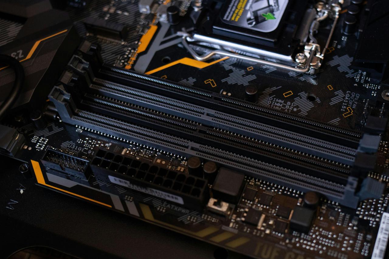
DDR5 Hardware Components and Memory Chips (Pexels)
DDR5 operates at 1.1 volts, a reduction from DDR4’s 1.2 volts, resulting in meaningful power savings per bit. Historically, power management was handled on the motherboard, but DDR5 integrates a Power Management Integrated Circuit (PMIC) directly onto the module, enabling configurable voltage ramps and current monitoring.
Unlike DDR4, all DDR5 chips include On-Die Error Correction Code (On-Die ECC), which detects and corrects storage errors before data is sent to the processor. This feature enhances reliability and enables the use of denser chips with higher per-chip error rates.
DDR5 is a dynamic random-access memory technology synchronized with the computer’s system clock. Unlike earlier SDRAM technologies, DDR memory performs data transfers twice per clock cycle—on both the rising and falling edges of the clock signal.
This method, known as “double pumping,” doubles the data transfer capacity without increasing the clock speed. In DDR5, the minimum burst length has been extended to 16, improving data bus efficiency and reducing the number of read/write operations needed to access the same cache line.
To ensure signal integrity required for high bandwidth, DDR5 employs Decision Feedback Equalization (DFE) technology. The integrated PMIC on the module configures voltage ramps and levels, enabling direct power management on the DIMM and reducing motherboard design complexity.
Compared directly with its predecessor DDR4, DDR5 exhibits clear advantages in speed, capacity, power efficiency, and architecture. While DDR4 reaches a maximum of 3200 MT/s, DDR5 starts at 4800 MT/s, increasing module bandwidth from approximately 25.6 GB/s for DDR4-3200 to 38.4 GB/s for DDR5-4800 and 51.2 GB/s for DDR5-6400.
In terms of capacity, DDR4 modules are typically limited to a maximum of 32 GB per module, whereas DDR5, thanks to higher-density memory chips and an updated architecture, supports up to 128 GB per module. Regarding power consumption, DDR4 manages power on the motherboard, while DDR5 modules include their own PMIC; additionally, the operating voltage has been reduced from 1.2 V to 1.1 V.
DDR5 has a notable latency disadvantage. Due to its looser timings, a standard DDR4-2133 C15 module offers approximately 5% lower latency than DDR5-4800 C40. This gap is only closed when DDR5 reaches 6400 MT/s. However, in bandwidth-sensitive workloads, a DDR5-6400 C36 configuration delivers 11% higher performance than DDR4-4000 C16.
There is no backward compatibility. Although both DDR4 and DDR5 modules have 288 pins, differences in keying position and pin layout prevent DDR5 modules from being inserted into DDR4 slots.

RGB-Lit Gaming System Interior — DDR5 Memory Modules (Pexels)
DDR5 has become the increasingly common memory standard in high-performance gaming systems. Intel’s processor series beginning with the 12th generation Alder Lake and continuing with the 13th generation Raptor Lake and 14th generation Raptor Lake Refresh all support DDR5. On the AMD side, Ryzen 7000 and Ryzen 9000 series processors based on the AM5 socket are designed exclusively for DDR5, making the transition to DDR5 mandatory for AMD users.
The impact of DDR5 on gaming performance varies by workload. In open-world games with large maps and high-resolution texture files, DDR5’s higher bandwidth accelerates data flow, improving frame rate consistency and reducing stuttering. In competitive gaming, this difference is relatively minor.
Memory speeds exceeding 6000 MT/s, enabled through XMP (Extreme Memory Profile) and AMD’s EXPO (Extended Profiles for Overclocking), deliver additional performance gains on AMD platforms by working in harmony with the processor’s integrated memory controller. As of 2025, DDR5 kits in the 6000–7200 MT/s range have become among the most popular configurations among gamers.
In server platforms, DDR5 has rapidly become the adopted standard for meeting the growing bandwidth and capacity demands of enterprise workloads. Intel’s 4th generation Xeon Scalable (Sapphire Rapids) and 5th generation Xeon Scalable (Emerald Rapids) processors, along with AMD’s EPYC Genoa and Bergamo series, are among the first major server platforms to support DDR5.
In server environments, DDR5 is also produced in RDIMM (Registered DIMM) and LRDIMM (Load-Reduced DIMM) formats beyond standard UDIMM configurations. RDIMMs allow more modules to be connected to the same memory channel through signal buffering, while LRDIMMs enable much higher capacities through load-reduction mechanisms. This allows terabyte-scale memory capacities in a single server system.
The importance of DDR5 in virtualization workloads is particularly evident. In hypervisor environments running multiple virtual machines on a single physical server, bandwidth can become a bottleneck; DDR5’s high bandwidth significantly alleviates this constraint.
With the rapid proliferation of large language models (LLMs) and deep learning applications, memory bandwidth has become a decisive performance factor in AI workloads. During the inference phase of an AI model, billions of parameters are continuously transferred from memory to the processor; in this process, memory bandwidth directly affects response time.
On CPU-based AI inference platforms—such as those based on Intel Xeon and AMD EPYC processors—DDR5’s bandwidth enables rapid loading of model parameters, reducing dependence on GPUs, especially for medium-scale models. Intel’s CPU-level AI acceleration instruction sets, such as AMX (Advanced Matrix Extensions), combined with DDR5’s bandwidth, deliver meaningful inference performance.
However, in large-scale AI training workloads, GPU memory technologies such as HBM (High Bandwidth Memory) and GDDR7 provide bandwidth far beyond what DDR5 can offer. Therefore, DDR5 serves as a complement to GPUs in the AI ecosystem, playing a critical role as system memory and for CPU-centric operations.

Data Center Server Racks (Pexels)
In data centers, DDR5 has become the preferred standard due to its advantages in energy efficiency and scalability. Thanks to the integrated PMIC on the module, power management is performed directly on the DIMM rather than the motherboard, offering significant benefits in energy savings and thermal management for large-scale deployments.
In terms of capacity, Micron and SK Hynix’s 1β (1-beta) technology-produced 128 GB DDR5 RDIMM modules represent a critical capacity threshold for intensive virtualization, large database systems, and real-time analytics workloads. In multi-socket server configurations, these modules enable the creation of terabyte-scale memory pools within a single physical system.
As of 2025, major cloud providers have adopted DDR5 as the dominant standard in their new-generation server infrastructure. In cloud services offering AI and machine learning, DDR5’s bandwidth and capacity advantages directly translate into improved service quality.

Data Center Server and Memory Infrastructure (Pexels)
Key advantages include high bandwidth reaching 51.2 GB/s at DDR5-6400, 128 GB capacity per module, reduced operating voltage of 1.1 V, standard On-Die ECC, and a dual subchannel architecture.
Primary limitations include higher latency compared to DDR4 due to looser timings, lack of backward compatibility with DDR4 slots, and the mandatory cost of platform upgrades to leverage DDR5.
DDR6 is currently under development by JEDEC as DDR5’s successor. LPDDR5 continues to extend its reach into mobile platforms. While DDR5 maintains its position as the primary standard for general-purpose computing, HBM and GDDR7 are taking center stage in AI and HPC domains.
Chan, Gibson. "RGB Aydınlatmalı Oyuncu Sistemi İçi — Lexar DDR5 Bellek Modülleri." Photograph. Pexels, 2024. Accessed May 14, 2026. https://www.pexels.com/photo/34301924
DDR5. "What's Legacy SDRAM? SDR VS DDR and What is the Difference?" Accessed May 14, 2026. https://ddr5.com/whats-sdram.html.
Faith New Dawn. "DDR, DDR2, DDR3, DDR4, DDR5, DDR6: Features, Applications." March 18, 2026. Accessed May 14, 2026. https://faithnewdawn.com/ddr-memory-technology-guide/
JEDEC. "Main Memory: DDR SDRAM." Accessed May 14, 2026. https://www.jedec.org/category/technology-focus-area/main-memory-ddr-sdram.
Kim, Dongkyun, Min-Su Park, Sungchun Jang, Jun-Yong Song, Hankyu Chi, Geunho Choi, Sunmyung Choi et al. "A 1.1-V 10-nm Class 6.4-Gb/s/Pin 16-Gb DDR5 SDRAM With a Phase Rotator-ILO DLL, High-Speed SerDes, and DFE/FFE Equalization Scheme for Rx/Tx." *IEEE Journal of Solid-State Circuits* 55, no. 1 (January 2020): 167-177. Accessed May 14, 2026. https://ieeexplore.ieee.org/abstract/document/8944229
Liu, Zhiye. "DDR5 Specification Released: Fast RAM With Built-In Voltage Regulators." *Tom's Hardware*, July 15, 2020. Accessed May 14, 2026. https://www.tomshardware.com/news/ddr5-specification-released-fast-ram-with-built-in-voltage-regulators
Matveev, Andrey. "DDR5 RGB RAM Modules on Bright Yellow Background." Pexels. Accessed May 14, 2026. https://www.pexels.com/photo/ddr5-rgb-ram-modules-on-bright-yellow-background-33384161/
Pexels. "Person Using Black Laptop." Accessed May 14, 2026. https://images.pexels.com/photos/1148820/pexels-photo-1148820.jpeg.
Historical Development
Technical Architecture
Frequency and Data Transfer
Channel Structure
Voltage System
On-Die ECC
Operating Principle
Differences from Previous Generations
Application Areas
Gaming Systems
Servers
Artificial Intelligence Systems
Data Centers
Advantages and Limitations
Advantages
Limitations
Relationship with Future Technologies
