


This article was automatically translated from the original Turkish version.
+2 More
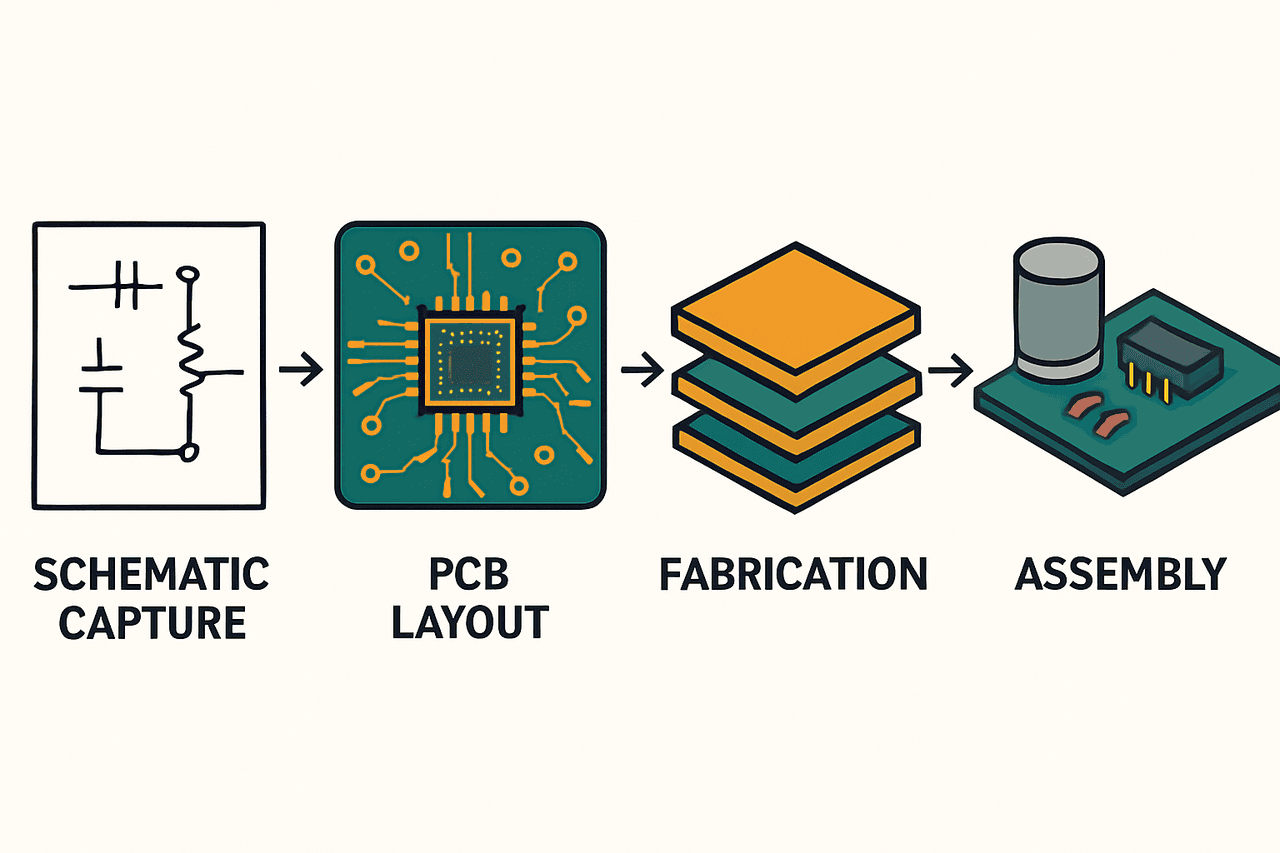
PCB Design (Generated with Artificial Intelligence)
PCB Design
Definition(s) | A plate containing conductive traces and pads used to mount electronic components and establish electrical connections between them. | ||||||||
|---|---|---|---|---|---|---|---|---|---|
Main Objective | To realize electronic circuits on a physical platform. | ||||||||
Design Output | Gerber files, Drill files, Bill of Materials (BOM). | ||||||||
Basic Stages | Schematic diagram, Component placement, Routing, Design rule check (DRC). | ||||||||
Common Material | FR-4 (glass fiber reinforced epoxy laminate). | ||||||||
Common Software | Altium Designer, KiCad, Eagle, DesignSpark PCB. | ||||||||
PCB (Printed Circuit Board), or its Turkish equivalent Printed Circuit Board, is a platform on which electronic components are mounted and electrical connections between these components are established through conductive pathways. PCB design is one of the most critical processes in transforming an electronic circuit from an idea into a physical product.
This process involves converting the schematic diagram of an electronic circuit into a layout plan that defines the physical placement of components and the routing of connections using copper traces. At the end of the design phase, a set of standardized data files known as Gerber files are generated, which are necessary for manufacturing the board. This process ensures that electronic devices are functional, reliable, and manufacturable.
PCB design is a multi-step process that transforms an idea or requirement into a tangible electronic circuit board. Each stage forms the foundation for the next and directly affects the quality, performance, and cost of the final product. This process is typically carried out using specialized computer-aided design (CAD) software.
Every PCB design begins with an idea that defines the functional requirements of the circuit. The first concrete step in the process is drawing the circuit schematic. A schematic is an abstract diagram that shows the electronic components to be used and their logical interconnections. At this stage, physical placement or component dimensions are not considered; the focus is solely on ensuring the circuit operates correctly from an electrical standpoint.
The schematic serves as the foundational blueprint for the design and acts as a reference for all subsequent steps. An error made during this stage can lead to major problems later in the process. Therefore, after the schematic is created, verification tests such as Electrical Rule Check (ERC) are typically applied to detect potential faults like open circuits, short circuits, or incorrect connections.
Once the schematic design is complete, the physical counterparts of each component in the circuit must be identified. This process involves creating or using component libraries. For each component, the library contains three essential elements: the schematic symbol, the PCB footprint, and optionally a 3D model. The schematic symbol represents the component on the schematic. The PCB footprint defines the physical dimensions and shape of the copper pads and mounting holes where the component will be soldered onto the board. The 3D model is used for mechanical checks and visualization.
Designers select components such as resistors, capacitors, and integrated circuits according to the project’s requirements and ensure that the footprint information is accurate. Selecting an incorrect footprint may prevent the component from being mounted on the board after manufacturing.
This stage is where the abstract circuit from the schematic is transformed into a physical board. The layout process includes defining the board dimensions, placing components, and routing the connections (traces) between them.
First, the board’s outer boundaries, locations of mounting holes, and any restricted areas are defined. Next, the layer stackup of the board is determined. For simple circuits, single-layer or double-layer boards are sufficient, while complex designs such as motherboards may have dozens of layers. The layer stackup includes not only signal layers but also power and ground layers. These specialized layers enhance signal integrity and reduce noise.
The placement of components on the board is critical for the circuit’s performance, manufacturability, and electromagnetic compatibility (EMC). A good layout is as much an art as it is a science. General placement guidelines include grouping related components (for example, separating analog and digital circuits), keeping high-frequency signal traces as short as possible, placing decoupling capacitors as close as possible to the power pins of the integrated circuits they supply, and positioning sensitive components away from board edges or noise sources.
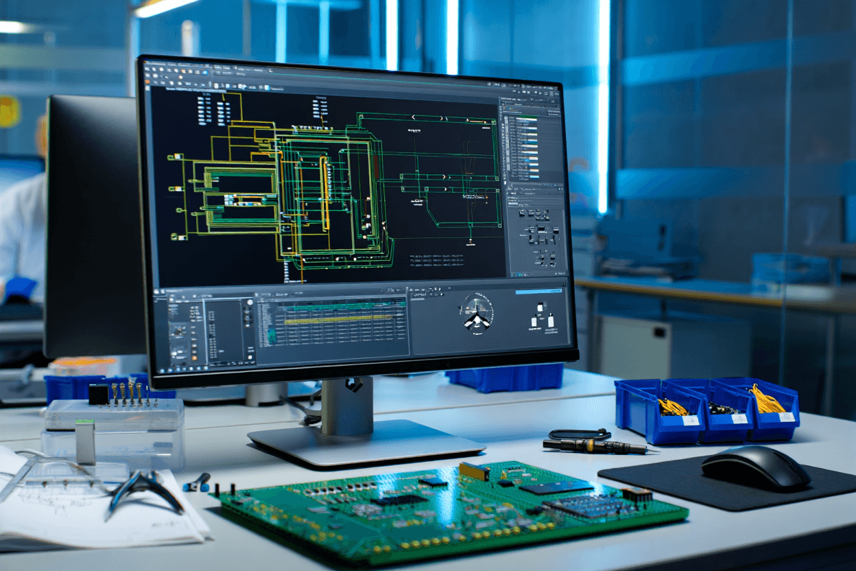
PCB Design (Generated by Artificial Intelligence)
After components are placed, conductive copper traces are drawn to realize the connections defined in the schematic. This process can be performed manually, automatically, or semi-automatically. During routing, parameters such as trace width, spacing between traces, and via (interlayer connection hole) dimensions are carefully considered. Trace width is calculated based on the current it must carry, while spacing between traces is determined to ensure electrical isolation. Special applications such as high-speed signals or RF circuits may require advanced routing techniques like impedance control or differential pairs.
To prevent manufacturing issues and electrical faults, a set of design rules is defined within the design software. These rules include constraints based on the manufacturer’s capabilities and the circuit’s electrical requirements, such as minimum trace width, trace-to-trace spacing, and hole sizes. In the final stages of design, a Design Rule Check (DRC) is run. The DRC scans the design against these rules and reports any violations, such as traces that are too close together or short circuits. The designer must correct all DRC errors before sending the design for production.
Once the design is complete and all checks have been performed, the final step is generating the files required by the PCB manufacturer. The industry-standard format is Gerber (typically RS-274X). Gerber files contain vector images of each layer (copper layers, solder mask, silkscreen). In addition, a drill file specifying the locations and sizes of holes, a Bill of Materials (BOM) listing the components and their specifications, and a pick and place file containing the position and orientation data of components for automated assembly machines are also generated.
PCBs can be manufactured in various structures and materials depending on application requirements.
The most commonly used insulating material is FR-4, a glass fiber-reinforced epoxy laminate. However, specialized materials such as Rogers are also used for high-frequency applications.
Various software tools are available for PCB design. These tools manage the entire process from schematic capture to layout design and generation of manufacturing files. Widely used professional software includes Altium Designer, Mentor Graphics PADS, and Cadence Allegro. For hobbyist or lower-budget projects, powerful free or low-cost alternatives such as KiCad, Eagle, DesignSpark PCB, and EasyEDA are available.
After the design process is complete, the physical realization of the board begins.
Before moving to mass production, a small number of prototypes are typically manufactured to test the accuracy and functionality of the design. This stage allows for early detection and correction of potential design flaws.
Approved Gerber files are sent to the PCB manufacturer. The manufacturer uses these files to create conductive traces, pads, and holes on copper-clad laminate boards through chemical and mechanical processes.
This is the process of placing and soldering electronic components onto the manufactured bare PCB. This can be done using through-hole technology (THT), where component leads are inserted through holes and soldered, or surface mount technology (SMD), where components are directly soldered onto copper pads on the board surface. The SMD process typically involves applying solder paste onto the board using a stencil, placing the components, and then reflowing them in a furnace.
The functionality of assembled boards is verified through various tests. During prototyping, needle-based test systems such as Flying Probe are used, while in mass production, functional tests are performed to confirm that the board operates as specified.
Khandpur, R. S. Printed Circuit Boards: Design, Fabrication, and Assembly. New York: McGraw-Hill, 2005.
Rahman, Ayesha, Marcus T. Nielsen, and Adebis Heritage Samuel. “Printed Circuit Board (PCB) Design and Electromagnetic Compatibility (EMC) Issues.” May 2025. Obafemi Awolowo University. Accessed July 8, 2025. https://www.researchgate.net/publication/392200304_Printed_Circuit_Board_PCB_Design_and_Electromagnetic_Compatibility_EMC_Issues.
Wei, Xue, and Xin Shu. “The Analysis and Optimization on Electromagnetic Compatibility for Printed Circuit Board.” *First International Conference on Information Sciences, Machinery, Materials and Energy*, January 2015. DOI: 10.2991/icismme-15.2015.271. Accessed July 8, 2025. https://www.researchgate.net/publication/300615558_The_Analysis_and_Optimization_on_Electromagnetic_Compatibility_for_Printed_Circuit_Board.
“ActiveBOM — BOM Management.” Altium Documentation. Accessed July 8, 2025. https://www.altium.com/documentation/altium-designer/activebom-bom-management.
“How to Create a Project Template.” *Altium Resources*. Accessed July 8, 2025. https://resources.altium.com/p/how-create-project-template.
“Preparing Your Design for Manufacture.” *Altium Documentation*. Accessed July 8, 2025. https://www.altium.com/documentation/altium-designer/preparing-your-design-for-manufacture.
“Schematic Capture.” *Altium Documentation*. Accessed July 8, 2025. https://www.altium.com/documentation/altium-designer/schematic-capture.

PCB Design (Generated with Artificial Intelligence)
PCB Design
Definition(s) | A plate containing conductive traces and pads used to mount electronic components and establish electrical connections between them. | ||||||||
|---|---|---|---|---|---|---|---|---|---|
Main Objective | To realize electronic circuits on a physical platform. | ||||||||
Design Output | Gerber files, Drill files, Bill of Materials (BOM). | ||||||||
Basic Stages | Schematic diagram, Component placement, Routing, Design rule check (DRC). | ||||||||
Common Material | FR-4 (glass fiber reinforced epoxy laminate). | ||||||||
Common Software | Altium Designer, KiCad, Eagle, DesignSpark PCB. | ||||||||
Stages of the PCB Design Process
Idea and Schematic Design
Component Selection and Library Management
PCB Layout Design
Board Definition and Layer Stackup
Component Placement
Routing
Design Rules and Verification (DRC)
Generation of Manufacturing Files (Gerber Files)
PCB Types and Materials
Design Software
Manufacturing and Assembly Processes
Prototyping
PCB Manufacturing
Assembly
Testing